 English
 Немецкий
 Арабский язык
 Французский
 Индонезийский
 Японский язык
 Корейский
 Японский
 Португальский
 Русский языкТекущий
 Испанский язык
 Тайский
 Турецкий
 Вьетнамский язык

Оборудование для чистых помещений
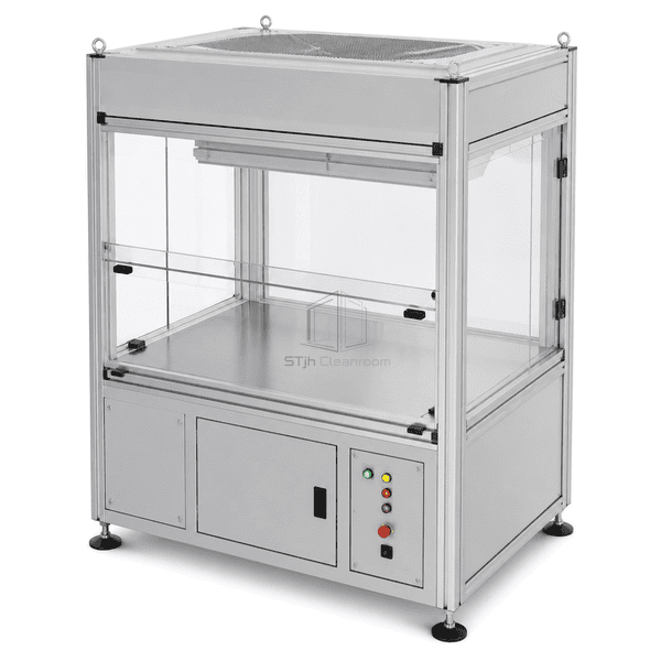
Semiconductor Mini-Environment
A compact process enclosure that creates a localized clean-air zone around sensitive semiconductor handling or inspection operations.
- Localized HEPA Airflow
- Transparent Process Access
- Low-Shedding Construction
- Configurable Tool Interface
Введение продукции
The semiconductor mini-environment combines an anodized aluminum frame, clear enclosure panels, an overhead fan-filter module and a cleanable stainless work deck. It separates the protected process zone from surrounding room traffic while preserving direct visibility and controlled operator access. Service panels, utility penetrations and equipment interfaces can be arranged around the installed tool, wafer handler or inspection fixture.
Основные характеристики
Clear panels maintain process visibility while limiting uncontrolled room-air entry.
Smooth metal work surfaces and low-shedding frame components support routine cleaning.
Modular access, controls and utility penetrations adapt to the enclosed process equipment.
Обеспокоенность клиентов продуктами
Localized wafer operations need stable cleanliness without enclosing an entire production bay to the same stringent conditions.
Room traffic can carry particles toward an exposed wafer-handling step.A filtered vertical airflow zone and physical enclosure shield the critical process area.
Opaque guards make it difficult to observe equipment and material status.Clear access panels preserve visibility from multiple sides without opening the enclosure.
A fixed enclosure can conflict with tool service and utility connections.Modular framing allows service doors, removable panels and penetrations to follow the actual tool layout.
Broad shadows and inaccessible corners complicate cleaning inspection.Smooth work surfaces and an open, visible internal layout reduce hidden residue traps.
Типичные приложения
Wafer inspection and metrologySemiconductor assembly operationsSensitive substrate handlingTool loading and process isolation
Технические параметры
Typical construction values for a modular semiconductor mini-environment are listed below.
| Основной материал | Anodized aluminum frame with clear polycarbonate panels and stainless steel work surfaces |
|---|---|
| Толщина панели | 6-10 mm transparent enclosure panels |
| эффективная ширина | 1200-2400 mm process enclosure width |
| Максимальная длина | Up to 3000 mm modular enclosure length |
| Толщина линий стали | 1.0-1.5 mm stainless steel work and cabinet panels |
| Плотность ядра | 2700 kg/m³ for aluminum framing and 7850-8000 kg/m³ for stainless components |
| Теплопроводимость | 14-17 W/(m·K) for stainless work surfaces |
| Поверхностная отделка | Natural anodized aluminum, clear glazing and brushed stainless steel |
| Объединенный тип | Bolted modular extrusion joints with gasketed removable access panels |
| Customization | Доступно в зависимости от предполагаемого применения и операционной среды. |
Доступные варианты
HEPA or ULPA terminal filtrationSliding or hinged access panelsIonization and task lightingTool-specific utility penetrations
Planning a Semiconductor Mini-Environment specification?
Отправьте нам ваши габариты, условия монтажа, целевые показатели производительности и требуемую отделку поверхности.