 ภาษาอังกฤษ
 ภาษาเยอรมัน
 ภาษาอาหรับ
 ฝรั่งเศส
 ภาษาอินโดนีเซีย
 ภาษาญี่ปุ่น
 ภาษาเกาหลี
 ภาษามาเลย์
 ภาษาโปรตุเกส
 ภาษารัสเซีย
 ภาษาสเปน
 ภาษาไทยปัจจุบัน
 ภาษาตุรกี
 ภาษาเวียดนาม

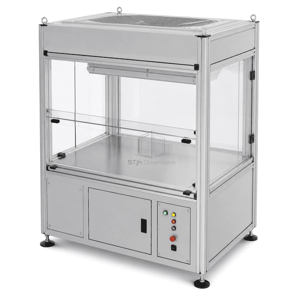
อุปกรณ์ห้องคลีนรูมเฉพาะอุตสาหกรรม
เซมิคอนดักเตอร์ Mini-Environment
A compact process enclosure that creates a localized clean-air zone around sensitive semiconductor handling or inspection operations.
- Localized HEPA Airflow
- Transparent Process Access
- Low-Shedding Construction
- Configurable Tool Interface
การแนะนําสินค้า
The semiconductor mini-environment combines an anodized aluminum frame, clear enclosure panels, an overhead fan-filter module and a cleanable stainless work deck. It separates the protected process zone from surrounding room traffic while preserving direct visibility and controlled operator access. Service panels, utility penetrations and equipment interfaces can be arranged around the installed tool, wafer handler or inspection fixture.
คุณสมบัติที่สําคัญ
Clear panels maintain process visibility while limiting uncontrolled room-air entry.
Smooth metal work surfaces and low-shedding frame components support routine cleaning.
Modular access, controls and utility penetrations adapt to the enclosed process equipment.
ความกังวลของลูกค้าเกี่ยวกับผลิตภัณฑ์
Localized wafer operations need stable cleanliness without enclosing an entire production bay to the same stringent conditions.
Room traffic can carry particles toward an exposed wafer-handling step.A filtered vertical airflow zone and physical enclosure shield the critical process area.
Opaque guards make it difficult to observe equipment and material status.Clear access panels preserve visibility from multiple sides without opening the enclosure.
A fixed enclosure can conflict with tool service and utility connections.Modular framing allows service doors, removable panels and penetrations to follow the actual tool layout.
Broad shadows and inaccessible corners complicate cleaning inspection.Smooth work surfaces and an open, visible internal layout reduce hidden residue traps.
การใช้งานทั่วไป
Wafer inspection and metrologySemiconductor assembly operationsSensitive substrate handlingTool loading and process isolation
พารามิเตอร์ทางเทคนิค
Typical construction values for a modular semiconductor mini-environment are listed below.
| วัสดุหลัก | Anodized aluminum frame with clear polycarbonate panels and stainless steel work surfaces |
|---|---|
| ความหนาของแผง | 6-10มม.แผงตู้โปร่งใส |
| ความกว้างที่มีประสิทธิภาพ | 1200-2400 mm process enclosure width |
| ความยาวสูงสุด | Up to 3000 mm modular enclosure length |
| ความหนาของเหล็กหันหน้า | 1.0-1.5 mm stainless steel work and cabinet panels |
| ความหนาแน่นหลัก | 2700 kg/m³ for aluminum framing and 7850-8000 kg/m³ for stainless components |
| การนําความร้อน | 14-17 W/(m·K) for stainless work surfaces |
| เสร็จสิ้นพื้นผิว | Natural anodized aluminum, clear glazing and brushed stainless steel |
| ประเภทร่วม | Bolted modular extrusion joints with gasketed removable access panels |
| การปรับแต่ง | สามารถใช้ได้ตามแอปพลิเคชันที่ตั้งใจไว้และสภาพแวดล้อมการทํางาน |
ตัวเลือกที่มีอยู่
HEPA or ULPA terminal filtrationSliding or hinged access panelsIonization and task lightingTool-specific utility penetrations
Planning a Semiconductor Mini-Environment specification?
ส่งมิติของคุณเงื่อนไขการติดตั้งเป้าหมายประสิทธิภาพและผิวที่ต้องการ