 日本語
日本語 ドイツ人。
ドイツ人。 アラビア語:アラビア語
 フランス語で
 インドネシア語
 日本語で。流れ
 韓国語
韓国語 マレー語
マレー語 ポルトガル語
 ロシア語
ロシア語 スペイン語
スペイン語 タイ語
タイ語 トルコ語
トルコ語 ベトナム語
ベトナム語

商品紹介
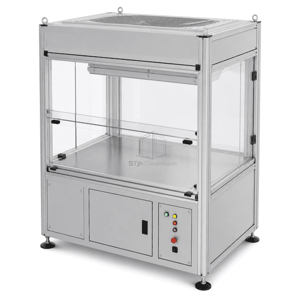
The semiconductor mini-environment combines an anodized aluminum frame, clear enclosure panels, an overhead fan-filter module and a cleanable stainless work deck. It separates the protected process zone from surrounding room traffic while preserving direct visibility and controlled operator access. Service panels, utility penetrations and equipment interfaces can be arranged around the installed tool, wafer handler or inspection fixture.
主要な特徴
Clear panels maintain process visibility while limiting uncontrolled room-air entry.
Smooth metal work surfaces and low-shedding frame components support routine cleaning.
Modular access, controls and utility penetrations adapt to the enclosed process equipment.
お客様の製品に関する懸念事項
Localized wafer operations need stable cleanliness without enclosing an entire production bay to the same stringent conditions.
Room traffic can carry particles toward an exposed wafer-handling step.A filtered vertical airflow zone and physical enclosure shield the critical process area.
Opaque guards make it difficult to observe equipment and material status.Clear access panels preserve visibility from multiple sides without opening the enclosure.
A fixed enclosure can conflict with tool service and utility connections.Modular framing allows service doors, removable panels and penetrations to follow the actual tool layout.
Broad shadows and inaccessible corners complicate cleaning inspection.Smooth work surfaces and an open, visible internal layout reduce hidden residue traps.
典型的な用途
Wafer inspection and metrologySemiconductor assembly operationsSensitive substrate handlingTool loading and process isolation
技術的なパラメータ
Typical construction values for a modular semiconductor mini-environment are listed below.
| コア材料 | Anodized aluminum frame with clear polycarbonate panels and stainless steel work surfaces |
|---|---|
| パネルの厚さ | 6-10 mm 透明エンクロージャパネル |
| 有効幅 | 1200-2400 mm process enclosure width |
| 最大長さ | Up to 3000 mm modular enclosure length |
| 鋼鉄の厚さを直面する | 1.0-1.5 mm stainless steel work and cabinet panels |
| コア密度 | 2700 kg/m³ for aluminum framing and 7850-8000 kg/m³ for stainless components |
| 熱伝導率 | 14-17 W/(m·K) for stainless work surfaces |
| 表面仕上げ | Natural anodized aluminum, clear glazing and brushed stainless steel |
| ジョイントタイプ | Bolted modular extrusion joints with gasketed removable access panels |
| カスタマイズ | 意図したアプリケーションと動作環境に基づいて利用できます。 |
利用可能なオプション
HEPA or ULPA terminal filtrationSliding or hinged access panelsIonization and task lightingTool-specific utility penetrations
Planning a Semiconductor Mini-Environment specification?
寸法、設置条件、性能目標、必要な表面仕上げをお送りください。