Contact Us
Are you planning a cleanroom project? Talk through the details with one of our experts. We’ll answer your questions and help you get started on a custom design.
Call Us
Call Now →
Email Us
Send Email Now →
Book A Meeting
Go to Calendar →
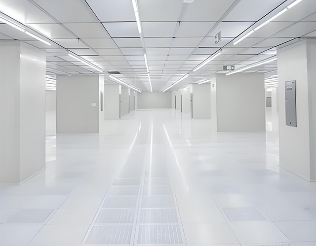
The future of tech lies in spaces that are unforgiving. Waferfab cleanrooms have been designed for the rigorous world of semiconductor fabrication, where a single particle can destroy years of R&D and millions of dollars in production.
These are more than just enclosures, they are performance-critical ecosystems engineered for precision, scale, and compliance. Whether high-volume fabs or pilot lines, the appropriate design allows wafers to seamlessly transition from process to process without contamination or disturbance.
Semiconductor fabrication requires absolute control. Each of these processes, from photolithography to etching and deposition, is vulnerable at a micro level, exposed to multiple sources of contamination, vibration, or static discharge. Without the right protections, production suffers, machinery breaks down, and your competitive edge disappears.
A semiconductor cleanroom provides the stable, ultra-clean environment necessary for today’s high-tech devices like CMOS, GaAs, GaN, and beyond. For companies committing serious dollars to wafer processing, the proper cleanroom is not a luxury. It is survival, especially in international markets.
Are you planning a cleanroom project? Talk through the details with one of our experts. We’ll answer your questions and help you get started on a custom design.
Call Now →
Send Email Now →
Go to Calendar →